StudentWiki:CrystalMolecularArchitecture
Crystal Molecular Architecture
Introduction
There are various crystal types:
- Metallic
- Covalent
- Molecular
- Macromolecular
- Large entities
- Quasicrystals (they don't have any translational symmetry, so are irrelevant for this course)
Crystal types - the basics:
- They involve all types of materials.
- Basic feature is an infinite repetition of a fundamental unit.
- Leads to atomic arrangements with well-defined symmetry and geometry.
- Similar principles apply at different length scales and complexities.
Historically it was recognised that the geometric shapes of crystals reflected a regular, repeating pattern of sub-units. Later this observation was confirmed experimentally, especially by X-ray and electron diffraction. To understand crystals we must first find a means to describe infinitely repeating structures.
Understanding the properties of solids is extremely important so as to apply their particular properties to various technological domains:
| Properties | Examples | Properties | Examples |
|---|---|---|---|
| MECHANICAL | Metals/Alloys, e.g. Titanium for aircraft Cement/Concrete, e.g. Ca3SiO5 Ceramics, e.g. clays, BN, SiC Lubricants, e.g. Graphite, MoS2 Abrasives, e.g. Diamond, Quartz |
OPTICAL | Pigments, e.g. TiO2 in paints Phosphors, e.g. Eu3+ in Y2O3 is red on TV Lasers, e.g. Cr3+ in Al2O3 is ruby Frequency-doubling of light, e.g. LiNbO3 |
| ELECTRICAL | Metallic Conductors, e.g. Cu, Ag.. Semiconductors, e.g. Si, GaAs Superconductors, e.g. Nb3Sn, YBa2Cu3O7 Electrolytes, e.g. LiI in pacemaker batteries Piezelectrics, e.g. α-Quartz in watches. |
MAGNETIC | Recording technologies - use of CrO2, Fe3O4 |
| CATALYSTS | Zeolite, ZSM-5 (a silicate), used for petrol refining. | SENSORS | Oxygen sensor, e.g. ZrO2/CaO solid solution. |
Some Definitions
Crystal = A solid form of matter showing translational periodicity in three dimensions in its atomic arrangement.
Crystal Structure = The arrangement of atoms in a single crystal.
Lattice = An infinite array of points in which each point is identical to every other.
Lattice Point = A point in the lattice which has identical surroundings to all the others.
Motif = The element of a structure associated with each and every lattice point (usually defined as a set of atomic coordinates relative to the lattice point).
Unit Cell = Unit cells represent a (minimal) component of the structure that reproduces the whole structure when repeated with purely translational motion (i.e., move through space but don’t rotate or twist!). Technically, you could use a primitive cell in all cases but this wouldn’t provide helpful symmetry information we need to visualise the cell.
Specifications:
- A unit cell is any parallelepiped (3D parallelogram) with lattice points at all corners.
- A primitive unit cell is a unit cell which contains only one lattice point.
- Non-primitive unit cell: a unit cell containing more than one lattice point (e.g., face centered, body centered, etc).
- Conventional unit cell: a unit cell chosen with a convenient relationship to the lattice symmetry (see point above about helpful symmetry information).
Lattice Parameters = Unit cell or lattice parameters are the lengths of the sides of the unit cell (a, b, c) and the angles between the unit cell axes (α, β, γ). Depending on the symmetry of the cell, some of the values may be identical (see later). The sides of the unit cell also define unit cell vectors a, b and c.
Lattice Vectors = Vector between two lattice points, written [UVW], defined in terms of the unit cell vectors as Ua + Vb + Wc. N.B. Minus signs are written above the relevant symbol and pronounced ‘bar’ to avoid confusion with a mathematical operation. E.g., [1 1 0] (see the Miller Indices section).
Graphite as an Example
2D Lattices in Graphite
Every infinitely repeating (tessellating) pattern can be thought of as a combination of:
- the pattern on the tile and
- the way in which the tiles are laid out
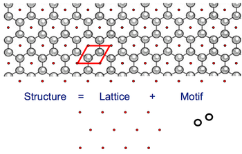
More properly, the infinite pattern (or ‘Structure’) is a combination of a local pattern (the ‘Motif’) repeated across an infinite set of ordered, identical points (the ‘Lattice’). The repeating unit is a ‘Unit Cell’ (the unit cell and the motif are not the same.) 2D example - a single layer of the graphite structure:
The process is reversible - given a structure you can find a motif and a lattice, given the motif and lattice, you can draw/imagine the structure.
- Lattice points are conceptual (no physical reality, they are NOT atoms)
- Lattice points do not have to coincide with any atoms, but for convenience are usually chosen to coincide with some.
- Their choice of location relative to the structure is arbitrary. The motif may be defined in many ways but, once made, the choice must be applied consistently.
For example, any one of the relationships between lattice and motif shown below would generate the graphite layer:
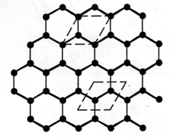
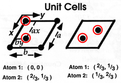
For 2D graphite, there are two possible unit cells, each with the same lattice but different motif:
Both structures are correct, despite their differences, thus reinforcing the fact that lattices and motifs are arbitrary - they are a means of analysing the repeating structure within a crystal structure.
3D Lattices in Graphite
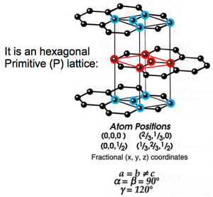
Graphite is actually a 3D structure. More specifically, it is a hexagonal primitive lattice.
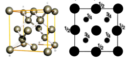
We often draw 3D structures in plan view (you must practise this). Fractional heights out of the plane are indicated numerically. If no number is written by an atom, it is in the plane of the paper. Because we are drawing a unit cell, an atom in the plane of the paper (height zero) must also appear at +1 (a whole number).
The calculation on the side of the diagram above is the ounting of the number of atoms contained within the unit cell.
This will be covered in a bit more depth in later sections, but basically:
- A vertex = ⅛ of an atom
- An edge = ¼ of an atom
- A face = ½ of an atom
- A body = 1 atom
Miller Indices - Indexing Directions
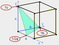
Sometimes it is necessary to express directions in crystals in a consistent way.
A direction index can be used to indicate this. Square brackets are used to indicate a direction vector.
So, for the example to the right:
- Select the plane closest to the origin (that doesn't pass through it).
- Determine the intersections of the plane on the axes of the unit cell.
- Express the reciprocals of ½, 1, 1 as integers and put them into round brackets (no commas).
- The Miller index is (211). The Miller index of all parallel planes is also (211).
Crystal Systems
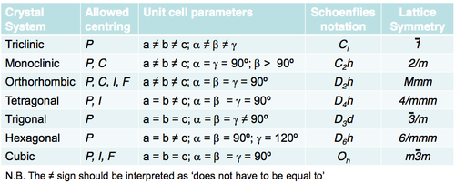
The Crystal System is the shape of the unit cell (see Bravais lattices). The Crystal System of a crystal may be referred to as ‘monoclinic’ but this is a type of shorthand. The real term should be the Lattice Symmetry name, ‘2/m’, which you will see much more if you continue in crystallography. Schoenflies notation is included in the following table and is good to describe individual objects within a lattice. Lattice Symmetry (Hermann-Mauguin notation) names are used for a collection of objects in a lattice.
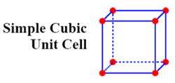
Simple Cubic Lattice Points:
Bravais Lattices
The hexagonal primitive lattice adopted by 3D graphite is one of only 14 Bravais Lattices which exist:
No need to learn them all - some of will become very familiar! The next one we will look at is the cubic primitive.
(N.B. The ≠ sign should be interpreted as ‘does not have to be equal to’)
Close-Packed or Not - Space Efficiency
In 1926, Goldschmidt proposed that atoms could be considered as packing in solids as hard spheres. Certain arrangements of these spheres lead to a maximised packing efficiency. These are termed close-packed structures and we will meet them shortly. Structures which do not meet this criterion are called non close-packed structures.
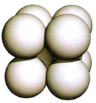
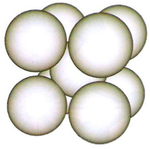
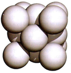
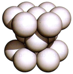
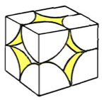
| CUBIC | BODY CENTRED CUBIC | FACE-CENTRED CUBIC | HEXAGONAL CLOSE PACKED |
|---|---|---|---|
 |
 |
 |
|
 |
 |
 |
|
Space efficiency: |
Space efficiency: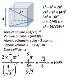 |
Space efficiency: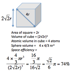 |
It is important to be aware as to how many atoms are contained within each unit cell:
- Vertex = ⅛ of an atom.
- Edge = ¼ of an atom.
- Face = ½ of an atom.
- Body = 1 atom.
Non Close Packed Structures
Primitive Cubic Structures
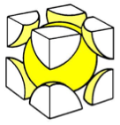
Primitive cubic structures are NON close packed - they have a space efficiency packing of 52 %.
In primitive structures such as these, there is only one lattice point, a point that repeats itself at each corner of the structure.
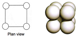
The plan view of a primitive cubic is:
Examples of primitive cubic structures are:
- α-Pollonium
- ReO3
- CsCl
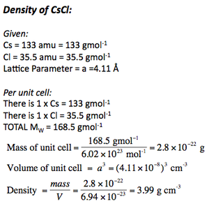
CAESIUM CHLORIDE
CsCl is an excellent example of a primitive cubic structure. There is exactly one caesium atom and one chlorine atom in each unit cell.
Each caesium and chloride has a coordination of 8, i.e. a coordination of 8:8.
This structure is also adopted by chlorides, bromides and iodides of larger cations, such as Tl+, NH4+.
The unit cell of CsCl is given below:
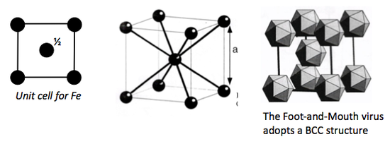
Body Centred Cubic
This is also a NON close packed structure, with a space efficiency packing of 68 %.
It is a structure commonly adopted by most metals, for example Iron (Fe).
IRON
It is important to realise the difference between BCC and CsCl's primitive cubic structure!
Caesium chloride is not a BCC structure, because the body of the unit cell is not the same atom as the corner atoms. CsCl is primitive cubic.
Each iron atom has a coordination to:
- 8 closest neighbours
- 6 second closest neighbours.
BCC isn't the only structure a metal can adopt.
Depending on the temperature and pressure conditions, a metal can adopt other close-packed structures; that we will discuss in the next sections.
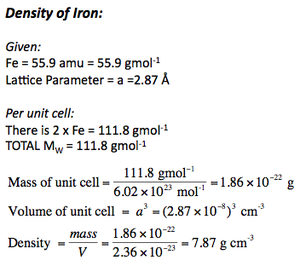
Calculating Densities
Calculating densities is important, and given the right data (molar masses and lattice parameter) it's possible to calculate it in few steps.
It is also important to be able to calculate the lattice parameters given the molar masses and the density.
Below are the density calculations for CsCl and Fe.
IMPORTANT = because densities are given in g per cubic centimetre, it is essential to convert lattice parameters into centimetres before cubing them.
- 1 nm = 10-9 m = 10-7 cm
- 1Å = 10-10 m = 10-8 cm
- 1 pm = 10-12 m = 10-10 cm
Close Packed Structures
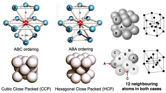
When packing spheres as efficiently as possible, there are two alternative ways of stacking the layers.
- Packing ABA leads to hexagonal close packed.
- Packing ABC leads to cubic close packed.
In both cases, the coordination around each atom is 12.
Under different conditions, the same solid can exist in different structural forms.
At STP, not all metals adopt the same structure.
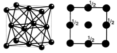
Cubic Close Packed: Face Centred Cubic
Cubic close packed (CCP) follows a specific arrangement of stacking in an ABC order that leads to a face centred cubic crystal structure.
It is the most theoretically efficient packing system of the crystal structures discussed so far, with a space packing efficiency of 74 %.
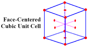
CCP structures are very common. Each atom is coordinated to 12 neighbours, with a total of 4 atoms in each unit cell.
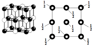
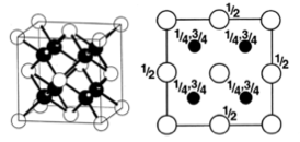
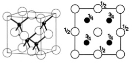
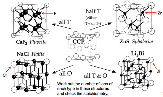
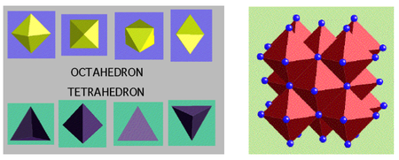
A very important aspect to keep in mind for the various CCP structures is which "holes" exist in the crystal structure - either octahedral holes or tetrahedral ones, or both.
(The holes are depicted by the white spheres in the diagram below - in other diagrams the white spheres just indicate a different atom).
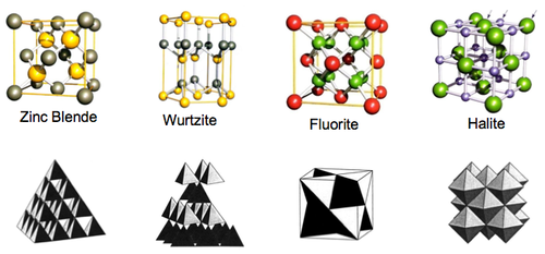
These are a few important cubic close packed structures to know and be aware of:
Below is a diagram summarising all the different FCC compounds and the way in which the crystal structure holes are occupied.
Hexagonal Close Packed
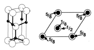
Hexagonal close packed follows an ABA packing sequence. This is another very common close-packed crystal structure, but is slightly harder to visualise compared to the CCP structure. The 3D and plan view of the structure and unit cell is given below.
The diagram with the bue and red lines, shows that three unit cells will fit next to each other within the hexagon, but it is important to note that despite having the same plan view, these unit cells will not actually make up the crystal structure of the material (or at least, not the correct representation). This is because unit cells cannot be rotated - only translated (moved about). Instead, it is better to view the hexagon as two unit cells, with two halves of two other unit cells slotted between them.
Once again, it is very important to be aware of the various "holes" within the HCP lattice.
There are both tetrahedral holes and octahedral ones, as was the case with the CCP structure.
The red lines and red atom help illustrate the environments of the Oh and Td holes.
Here are the most important hexagonal close packed structures to be aware of:
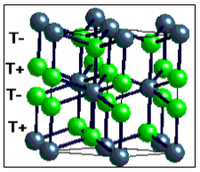
Interestingly, there is no hexagonal close packed analogue of the cubic close packed Fluorite structure.
There is simply no HCP compound known in which all the tetrahedral hols are populated, due to the amount of steric strain and lack of space available within the structure.
There are compounds known with half the Td holes filled (either T+ or T-) but not all filled. A compound with all Td holes populated would give this:
Calculating Densities
From all these details we can already start calculating densities, given the correct starting information.
Ionic Solids
Clearly the first major determinant of possible structure types is the stoichiometry.
For an AB system (e.g. NaCl), only structures are possible in which the coordination numbers of A and B are the same (so NaCl could not take the CaF2 structure).
Principles of Laves:
- 1.Space principle – space is used most efficiently
- 2.Symmetry principle – highest possible symmetry is adopted
- 3.Connection principle – coordination numbers are maximised
These are followed well by metals and the inert gases (close-packed structures). Deviations include the BCC metals (see earlier slide) and where there are ‘preferred interactions’ (e.g., square planar metal environments, metal-metal bonding, accommodation of lone pairs), which can go against the above principles:
Different Representation
Obviously knowing where the atoms are exactly is the most useful way of representing a crystal.
Nevertheless, it is always quite interesting to represent the structures more "spacially", or according to the corners and faces occupied.
So for example:
Which leads to this, for the compounds discussed:
Crystal Defects
"Crystals are like people, it is the defects in them which tend to make them interesting!"
- Colin Humphreys.
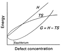
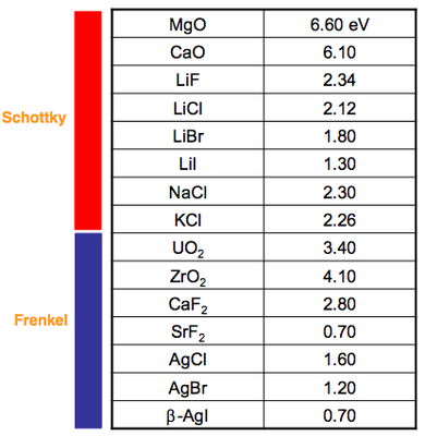
Real crystals are not perfect. In fact, there is an entropic driving force that creates a thermodynamic equilibrium for a concentration of defects to exist throughout a structure. Defect energies vary widely, depending on the crystal and leading to different concentrations. The table on the right shows the enthalpy of formation of the lowest energy defect (i.e., dominant one) in a range of materials.
Crystal defects are extremely important when considering the macroscopic properties of a solid. For example, when buying a diamond it's usually the number and type of defect(s) present that determine its purity and price for a certain crystal size. Or, another example would be the production of advanced silicon-based semiconductors where very pure silicon crystals are requires as the starting material. A very specific amount of defects are then introduced into small areas of the sample that allow it to adopt certain properties.
There are different types of crystal defects:
- 0D - Point defects (single atoms): for example, vacancy, substitutional, interstitial defects. This is the most common type of defect for a crystal with a regular lattice structure. Point defects (vacancies) usually increase in frequency as the temperature is increased. Having vacancies present within a structure allow for mass ion transport to occur once a suitable concentration of defects has been achieved. To calculate the number of point defects present within a crystal, this formula is used:
- where n = number of defects per unit volume
- where N = number of cation and anion sites
- kB = the Boltzmann constant
- T = temperature
- ΔH = the enthalpy required to create a vacancy in a perfect crystal
- 1D - Dislocations: Dislocations are line-defects, which means that the interatomic bonds are significantly distorted only in the immediate vicinity of the dislocation line. This area is called the dislocation core. Dislocations are able to create small elastic deformations of the lattice at large distances.
- 2D - Planar defects: Shear planes, stacking faults, grain boundaries form a class of planar defects. These originate from the fact that single crystals are rarely found in real materials unless the growth conditions are specially designed and controlled. Instead, solids generally are made up of a number of small crystallites or grains all packed together. The grains can be from nanometers to millimeters in size and the orientations of atomic planes are rotated with respect to the neighbouring grains. These materials are called polycrystals and the individual grains are separated by grain boundaries. These are regions of less densely and regularly packed ions as compared to the bulk of the grains.
Intrinsic Defects
Intrinsic defects preserve the stoichiometry and composition of the material.
To preserve charge neutrality, defect pairs are common, the two main types of which are:
- Schottky defects
- Frenkel defects
The ones for which the dominant (lowest energy) defect is the Schottky type are highly ionic.
The ones denoted as having Frenkel defects have highly polarisable ions and tolerate interstitial species.
The concentration of defects varies considerably between compounds. For example:
- NaCl there might be one defect per 1014 formula units
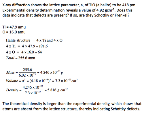
- TiO can have has much as one defect per 10 formula units.
Density calculations can give us an idea as to what defect is present in a crystal. Examples are demonstrated below:
Extrinsic Defects
Extrinsic defects involve change of stoichiometry and/or the introduction of another species. Most simply, homovalent or neutral additions of other elements do not change stoichiometry but form solid solutions (solid phases with continuously variable composition within a certain range). They may be of two types:
- Substitutional solid solutions
- Interstitial solid solutions
Ruby exemplifies a substitutional solid solution whereby Al3+ is substituted by Cr3+ in the structurally similar solids Al2O3 and Cr2O3.
Note the large range of x! The reaction for this substitutional solid generation is given below.
A good example of an interstitial solid is hydrogen dissolved in Pd. This finds applications in the separation of hydrogen from other gases using the membrane shown below.
Simple AB oxides (and other binaries) fall into a number of categories.
Extrinsic defects in binary systems can change stoichiometry. What actually happens depends on the nature of the material. Four examples:
On oxidation of the metal, either the extra oxide anions occupy interstitial sites or the oxygen is combined into the lattice, extending it so that cationic vacancies result (run out of metal). On reduction the reverse is true when oxygen is removed, resulting in either cations occupying interstitial sites or anion vacancies in the lattice (oxygen deficient).
Doping and Electronic Properties
Doping of heterovalent ions introduces further defects. It involves the deliberate addition, usually in very small amounts, of foreign dopant atoms.
This is a common method of modifying defect concentrations and hence properties - especially in semiconductors (see the electronic properties of solids course).
In most cases, the dopant atoms take the place of the original atoms within the crystal lattice.
- Higher valence cations: cation vacancies OR interstitial anions.
- Lower valence cations: anion vacancies OR interstitial cations.
Doping of conventional semiconductors is familiar, but changes of stoichiometry can also change electronic character.
In conventional semiconductors, orbital overlap is good, bands are broad and electrons move easily.
If orbitals are tightly bound (e.g.,TM d-orbitals) and delocalisation weak, bands will be narrow. "Hopping" then becomes an important electron transport mechanism.
- Zn1+xO is an n-type semiconductor.
- NiO (pale green insulator) becomes Ni1-xO (black p-type semiconductor)
- LiCoO2 can lose Li+ to give p-type Li+1-xCo3+1-xCo4+xO2
Mass Transport of Ions and Ionic Conductivity
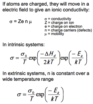
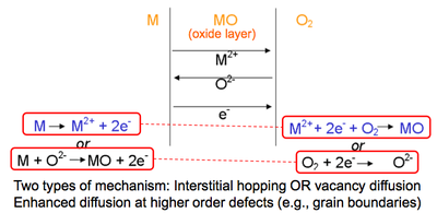
The presence of defects (especially of vacancy defects) enables atomic motion, either through interstitial or vacancy diffusion. Higher order defects (especially dislocations and grain boundaries) enhance diffusion paths. Needless to say, higher temperatures favour diffusion by increasing defect concentrations and mobility. Diffusion is crucial for solid state reactions. One simple example is the oxidation of metals:
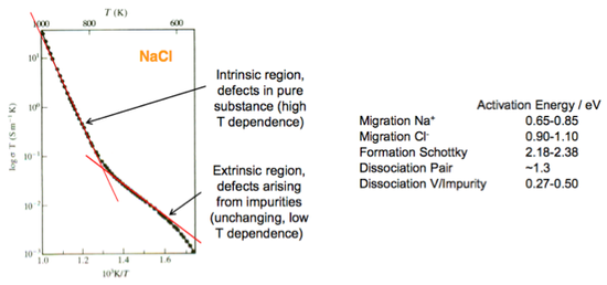
If atoms are charged, they will move in a electric field. Thus, as well as diffucion being possible, we can also force ions to move within a lattice. This leads to ionic conductivity.
The most important formula are shown in the diagram opposite. An example of a graph of ionic conductivity is also given below. From it we can identify the extrinsic and intrinsic regions.
Grain Boundaries
Real crystals are finite - they have external surfaces (of varying types). Most crystalline materials are not single crystals but many individual crystals (or ‘grains’) randomly jammed together in different orientations.
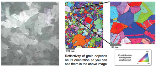
Such materials are called ‘polycrystalline’, with 2D defects between the grains, called ‘grain boundaries’. Grains are often microscopic but there are visible ones, for example in galvanised (Zn-coated) steel. Each grain is around 1 cm in this case (below left). All metals are polycrystalline but grains are usually too small to see.
Grain boundaries are important for many properties, including for example, diffusion effects discussed earlier.
Metal turbine blades are made of a single crystal (e.g., Ni) to avoid diffusion of Ni metal that occurs at grain boundaries in high temperature environments.
Grain boundaries are important in several ways. They create paths for atoms to diffuse into the material, and they enable the scattering of light passing through transparent materials to make them opaque. They also affect mechanical properties because they limit the lengths and motions by which a dislocation can move. This means that smaller grains (and consequently more grain boundary surface area) strengthens materials. The size of the grains can be controlled by the cooling rate of a sample when it is produced from the melt. Generally, rapid cooling produces smaller grains whereas slow cooling results in larger grains. At room temperature large grains generally result in low strength, hardness and ductility.
Dislocations
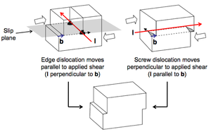
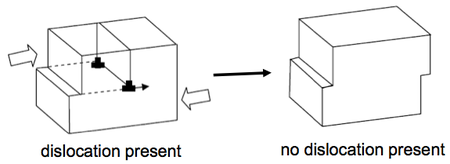
Dislocations can be introduced and thought of as extra lattice planes inserted in the crystal, but not extending through all of the crystal but ending in the dislocation line. Motion of dislocations allows slip – plastic deformation when interatomic bonds are fractured and reformed. Actually, slip always occurs through dislocations motion. Dislocations are defined in terms of:
- a line vector (l)
- a Burgers vector (b).
The line vector indicates the direction of the dislocation ‘core’ (the centre of the defective region). The Burgers vector indicates the displacement of the crystal after the passage of the dislocation. The slip plane is the plane over which the dislocation moves.
Intercalation Compounds
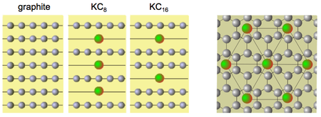
Layered compounds can accept atoms/ions that ‘intercalate’ between the layers. The classic examples are graphite intercalation compounds:
Ionic transport of potassium ions occurs through the ‘corridors’ formed while the electrons are transported through the graphite.
Lithium ion batteries function by shuttling lithium ions from LiCoO2 (shown on right) to graphite and back again.
